Hi again

This may get a little off-topic and even more techie at some parts.
This is a "spin off" thread from
this thread.
The idea is to build an interface for the model1 comm board to do some "blackbox" testing.
For the sake of simplicity, I choose the IBM PC's ISA-bus, as it features a lot of control logic that we need.
The basic idea is to use a (rather) small I/O area to access the model1 comm boards "host" port.
Logic - IdeasThe model1 comm board features an 21 bit address bus (A0 to A20) and 16 bit data bus (D0 to D15), there are several other control signals, as IOW-, IOR-, VINT-, EX1- and EXWAIT-.
And of course there is a 32M pin for the 32MHz OSC on the model1 cpu board.
I came up with a rather simple "glue" logic.
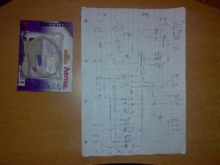
(please note - this image is neither correct nor complete
)
HardwareThe model1 comm board features an 21 bit address bus (A0 to A20) and 16 bit data bus (D0 to D15).
These 21 address bits are grouped:
- A0 to A12
- A16 to A20
A1 to A11 are connected to the shared memory chips - nothing special about it.
A1, A12, (A0 or A16), (A17 or A18), A19, A20, EX1-, IOR- and IOW- are connected to IC6 - a PAL18 which serves as address decoder.
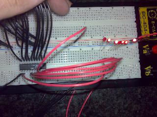
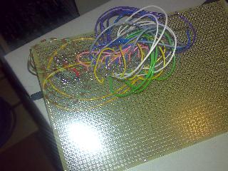
So the idea was to read out the PAL and check what it does... I don't get that JEDEC stuff, so I used a rather "hacky" approach - with breadboard and some wires
As it turns out - A16 to A19 need to be "low", A20 and EX1 need to be "high" - to select the comm board in any way.
The comm board is "mapped" in the model1 address space at 0xB00000 so we can guess which address bits would be used.
HEX     BIT
B00000  1011 0000 0000 0000 0000 0000
...
B01000  1011 0000 0001 0000 0000 0000
...

        2222 1111 1111 1100 0000 0000
        3210 9876 5432 1098 7654 3210
           + ----    x xxxx xxxx xxxx
That leads to this:
Read  @ B00000 = MEMR
Write @ B00000 = MEMW
...
Read  @ B00FFF = MEMR
Write @ B00FFF = MEMW
Read  @ B01000 = CNRD (Bit0)
Write @ B01000 = CNWR (Bit0)
Read  @ B01002 = FGRD (Bit0 & Bit7 [ZFGWR])
Write @ B01002 = FGWR (Bit0)
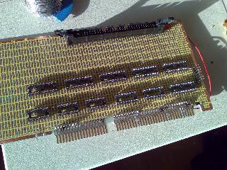
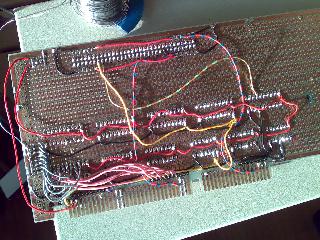
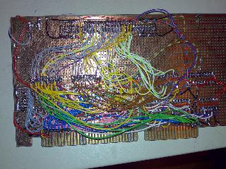
Bridgeboard - ISA sideThe bridgeboard is rather simple.
For the 32MHz signal I used a 32MHz OSC... quite simple huh?

I use a 74682 as "chip select" decoder for the ISA-bus.
P-Signal use A3 to A9 and AEN signals.
Q-Signal uses 7 Jumpers and GND.
If P equals Q we know our bridge is accessed - IOCS- goes "low".
I also use two 74138 as read- and write-address decoder.
ABC-Inputs are connected with A0 to A2.
G2A- is connected to CS-.
G2B- is connected to IOR- / IOW-.
I only use the Y0- and Y2- outputs - W0-/W2- and R0-/R2-.
As this is a 16 bit capable card, I need to pull down IOCS16-.
Also, if the comm boards memory is "busy", I need to pull down IOCHRDY.
For that, I use a 74125 and a 7432.
CS- is used to connect IOCS16- to GND.
(CS- or EXWAIT-) is used to connect IOCHRDY to GND.
This works because both signals CS- and EXWAIT- need are "active low", and the OR-gate output gets "low" only if both inputs are "low" too.
As for some other control signals.
The ISA-bus has a RESET signal, and the model1 comm board uses a RES- signal.
I simply invert the signal using an 7404.
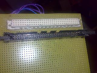
To latch the address, I use two 74273.
W2- signal is used to "update" the latched address.
the outputs are connected to the comm boards address lines A0 to A15
As I don't have any VSYNC signal on the ISA bus I choose to use R2- as VINT- signal. More on this one later.
W0- is connected to the comm boards IOW- line.
R0- is connected to the comm boards IOR- line.
I
planed to generate a valid EX1- signal like this:
W0- and R0- get inverted by the 7404, both signals are then fed to the 7432 - the ORed result is then inverted again (7404) and thus used as EX1-.
However, in the end I became lazy and simply connected EX1- to GND
The data lines are connected to both the 74273 inputs as well as the comm boards data lines D0 to D15.
At first I used two 74645 bus gates - however I removed them later as they are not needed.
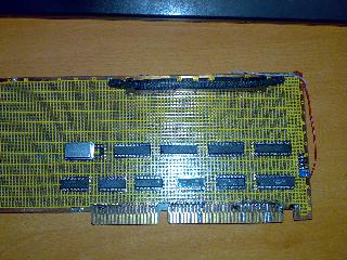
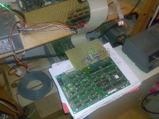
At last... nothing blew up after plugin it in for the first time

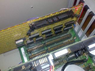
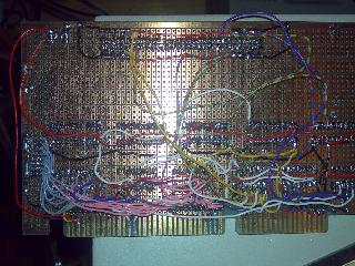
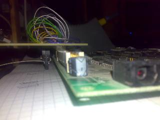
Bridgeboard - model1 comm board sideThe "other" side of the bridge is a simple (still messy) wire adapter.
It simply plugs into the comm board
(Phew... nothing blew up
)
Software sideAs for the PC side, the bridgeboard is located at IO 0x300 to 0x307:
Writes to 0x302 update the address latches (16 bit).
Reads from 0x302 trigger a VINT-. (theoretical - should be about 58hz?)
Reads/Writes to 0x300 are processed by the comm board.
So if I want to read data located at 0x0123 from the comm boards shared memory...
I write 0x0123 to 0x302 and then read from 0x300.
One thing I didn't actually pay attention to, is the endianess. My Intel CPU (as well as the comm boards Z80) use little-endian. However I don't know what the NEC V60 used on the model1 cpu board does.
I did some simple tests routines (in Visual Basic ^^) to check the bridgeboard.
I can access both CN (0x1000) and FG (0x1002) "registers" without problems.
My SRAM test (reads and writes from/to 0x0000 to 0x0FFF) indicates that this is working too - however the memory at 0x0000 always returns 0xFF.. which I suppose gets writen there by the comm boards Z80.
*UPDATE*
Turned out the SRAM was accessed to fast, took that into account when writing, now everything works.
*UPDATE2*
VINT- didn't work as intended, the ISA IOR- signal is "too short" for the Z80 to recognize as interupt. Using the VGAs (negative) VSYNC for now.
*UPDATE3*
Linking up works
Now I need to visit a friend and "hook" this thing into a real Virtua Racing network


 Home
Home Help
Help Search
 Login
Login Register

 Send this topic
 Print
Print Topic: (slightly off-topic) Using the Model1 Comm-Board with a PC :D (Read 2526 times)


